Making fine pitch PCB prototypes with fiber laser
There are quite a lot of inexpensive and fairly reliable PCB manufacturers that can produce double-sided PCB’s with solder-mask and silkscreen in a day or two, but what if you need it now? I will not cover expensive prototyping machinery nor messy printer/etching process instead let’s use a 20W Fiber laser. Because… who does not like lasers, right?
Goal
The ultimate goal is to have a soldered fine pitch (0.1mm/4mill track and clearance) component as fast as possible (30min) along with a few passive components.
The material of choice is common FR-4 with 0.018 or 0.035mm copper thickness. It would be perfect to have double-sided routing, but via copper plating process complexity and time restriction imposes limits to single-sided design without drilling (though with some drawbacks it can be done).
Design preparation
Gerber files
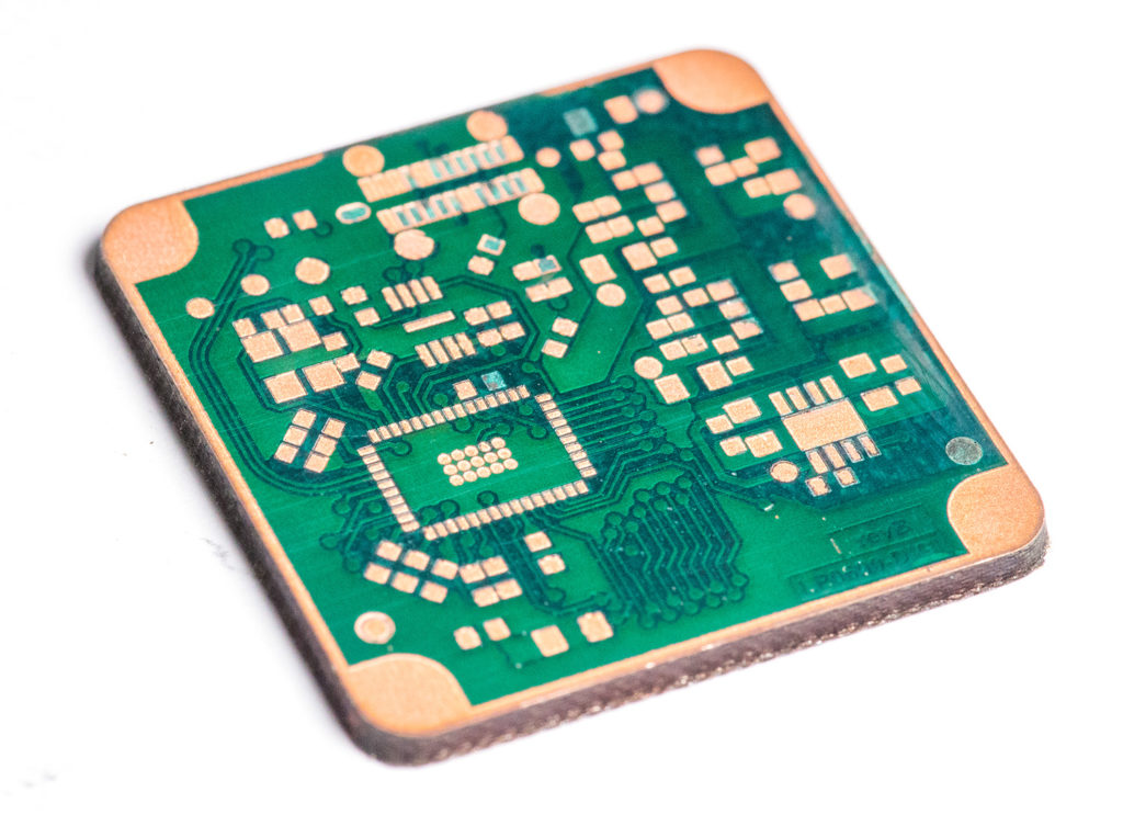
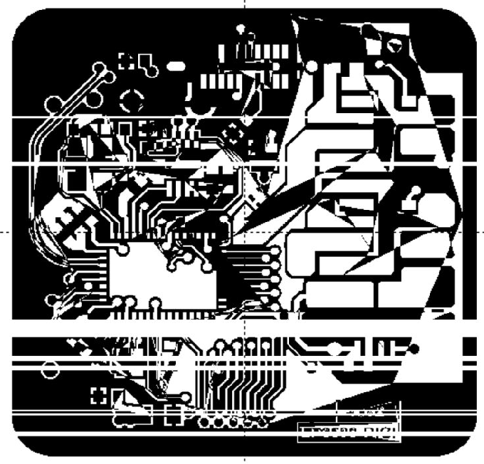
For this experiment, I used one of the fresh upcoming camera design. Skipping Gerber export step as it varies from software to software. For this test prepare 3 Gerber files:
- TOP tracks layer
- TOP Solder-mask layer
- Contour layer
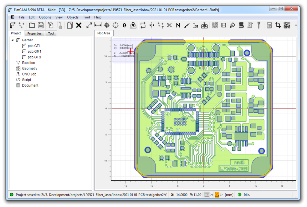
FlatCam import
FlatCAM lets you take your designs to a CNC router. You can open Gerber, Excellon or G-code, edit it or create from scatch, and output G-Code. Isolation routing is one of many tasks that FlatCAM is perfect for. It’s is open source, written in Python and runs smoothly on most platforms.
http://flatcam.org/
FlatCam is also an ideal tool to prepare DXF/DWG vector files for further processing. Feel free to explore this powerful and open-source tool.
- File / Open / Open Gerber… and load all prepared files
- Double click on each Gerber layer and generate Isolation Routing layers
- Double click on each Geometry layer and Generate CNCJob object
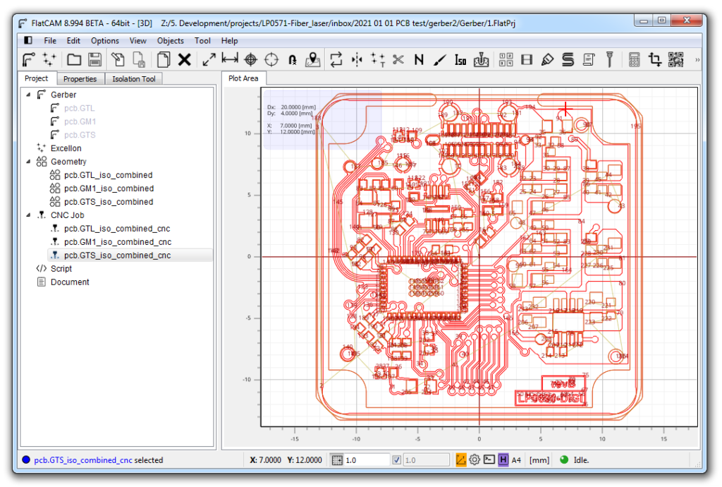
Then export each CNC job layer to an SVG file. Here we go, Gerber files were converted to more usable DWG files that can be used by EZCAD software.
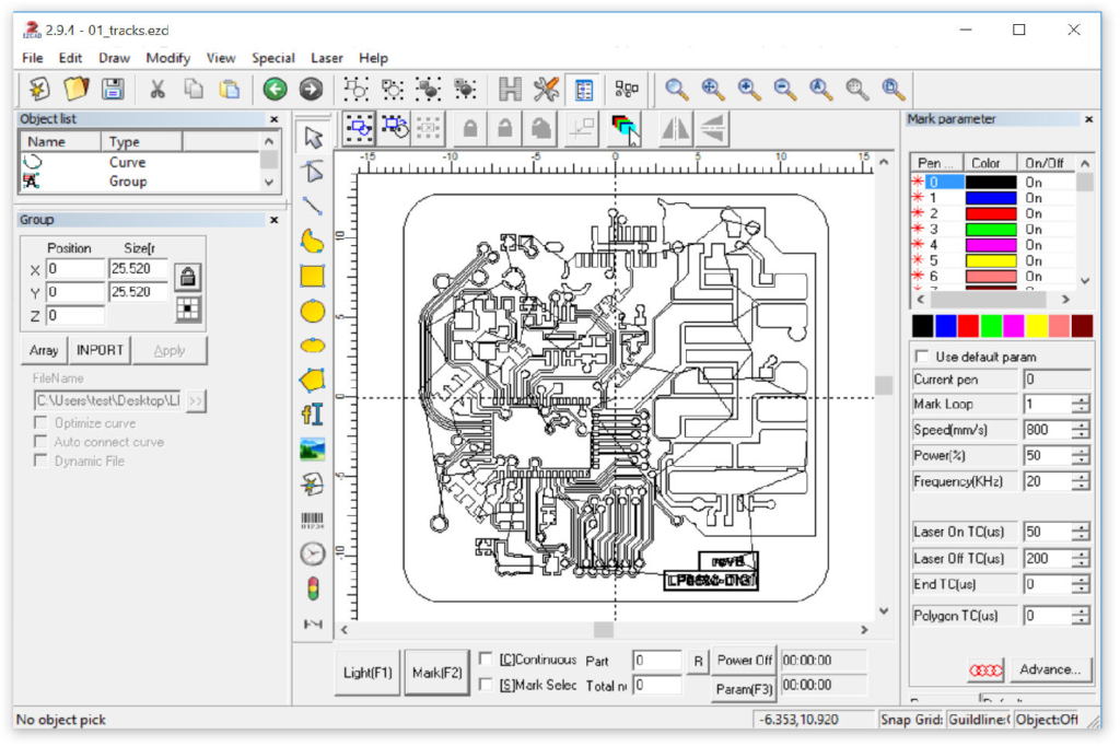
EZCAD import
LIT Laser systems represents the latest in smart fiber laser technology. Our approach has drasticly reduce the price of laser systems. This unprecedented value and versatility has enabled students, technicians, engineers, inventors, makers, and hobbyists a chance to own laser systems that have been out of reach for many.
https://www.litlaser.com/ezcad
EZCAD comes with the vast majority of laser marking machines and is considered a de-facto tool. Unfortunately has some imperfections (actually tons of them). One of the major ones – outdated and buggy vector file importer. So after opening the top layer we will see a broken image (which is easy but tedious to fix)
Make copper traces
First, let’s fix the vector file imported in EZCAD. Here is the workflow that worked:
- Select all geometry
- Click Edit / UnGroup
- Select each jump line and delete. I know this is tedious work, but could not find any quick workarounds
- Click Edit / Group
This is another nasty EZCAD bug – if you would apply hatching now, geometry will be totally messed up.
- Quick workaround – Click Modify / Curve Edit / Auto Connect (0.010mm) and geometry hatching looks better (might need grouping / ungrouping step)
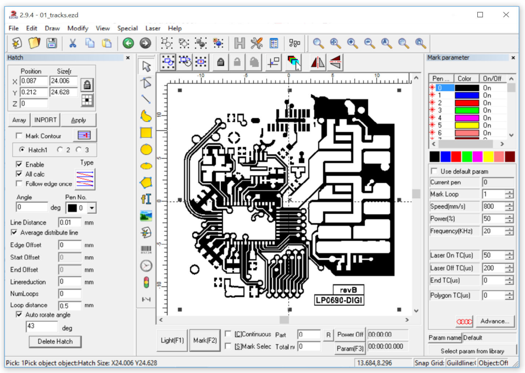
For track isolation use hatching and laser parameters like in the screenshot above. Not ideal, but should be good to start experimenting.
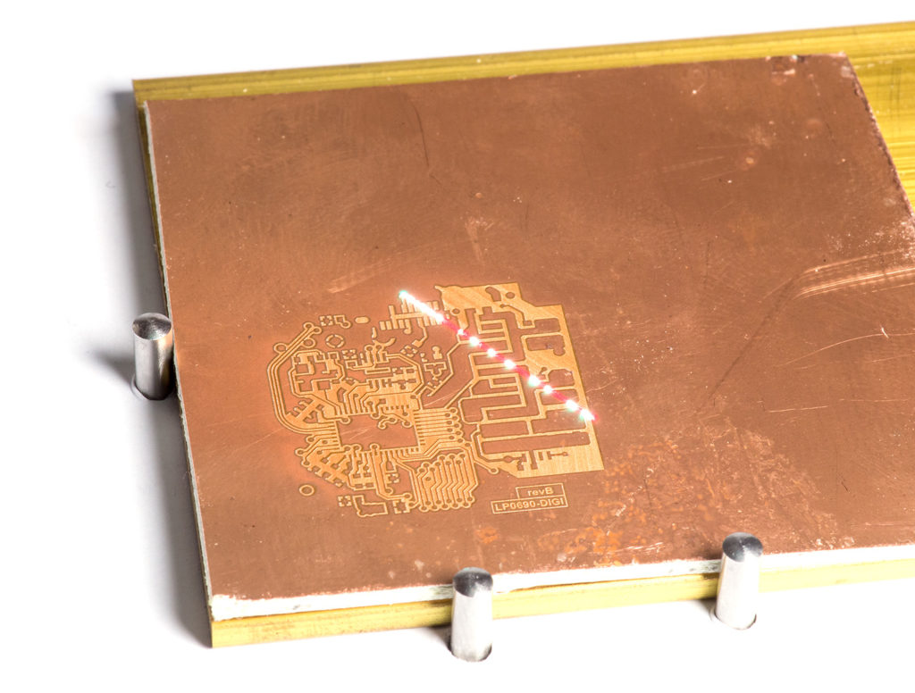
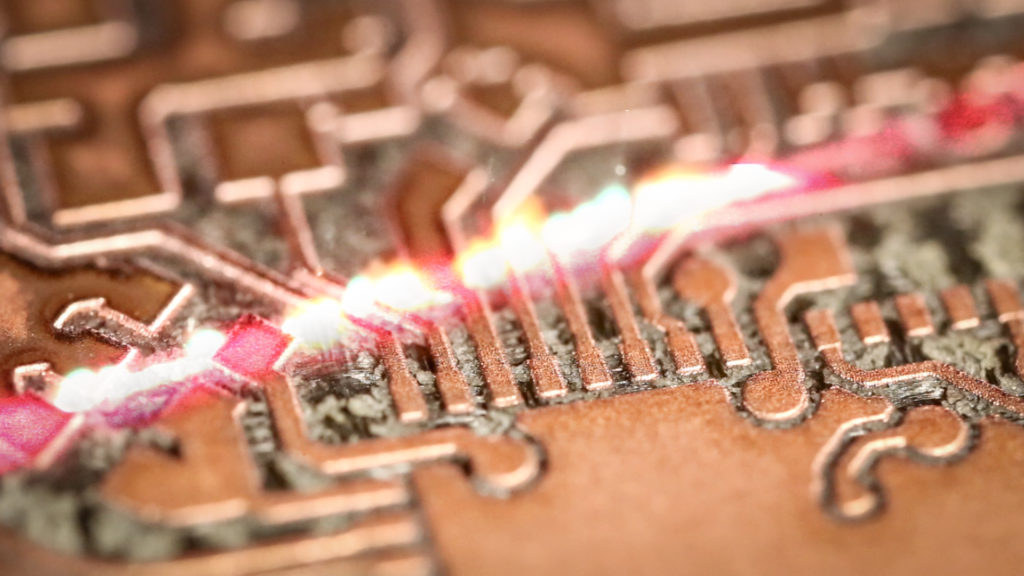
It took about 20 cycles to cut through 0.035mm copper foil. Some of these passes were with increased power to 90% to speed up the material removal rate. A good hint when to decrease laser power is to observe copper color – with decreased layer thickness it will heat up more and change color. 50% of power will not greatly damage the substrate, while higher power settings make resin burn.
Prepare soldermask layer
Use PCB UV Curable Solder Repairing Paint (also good choice Dynamask 5000 dry film)
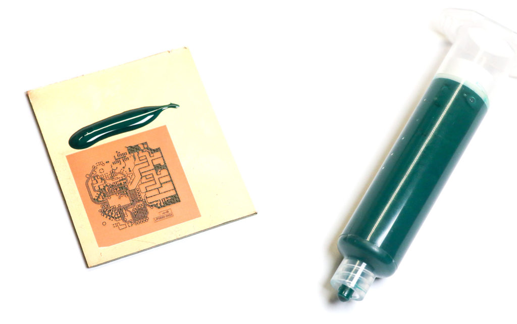
- Spread the paint evenly on the PCB (use a thick transparent plastic sheet and rubber roller to spread evenly)
- Make sure there are no bubbles
- Introduce to 365nm UV light to cure. This should take a few minutes, for exact timing read material specifications, and experiment.
- The protective sheet should peel off without damaging the freshly cured solder mask
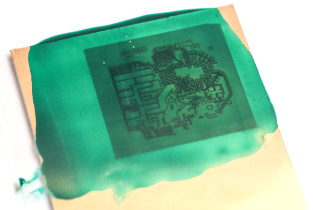
More or less evenly spread and cured solder mask. This forms a pretty resistant layer that can withstand soldering in high temperatures.
Open solder mask
Rinse and repeat importing solder-mask layer into EZCAD software.
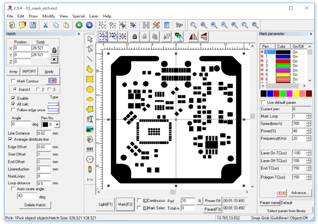
Laser settings in screenshot above. Depending on your layer thickness several passes will be required.
Cut PCB contour
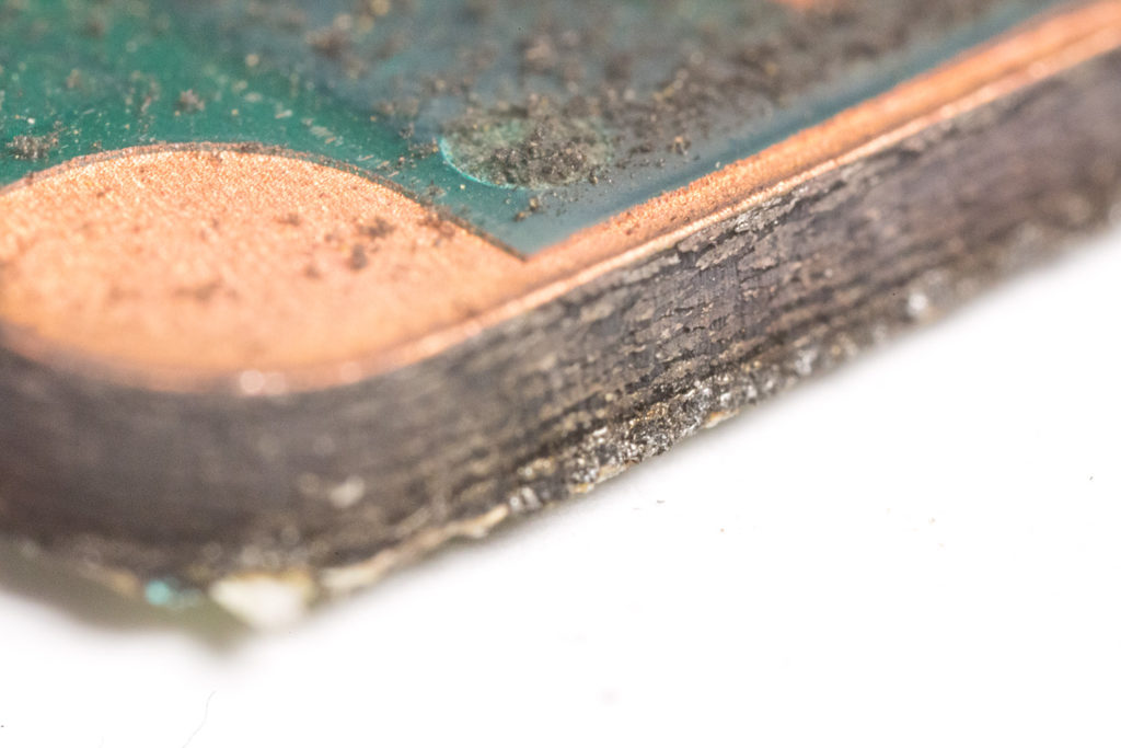
The final step is to cut PCB out of stock material. A laser will not warp and skew FR-4 material so this is a very nice way to have PCB made to size. It will burn edges though, but light touch with 400 grit sandpaper will fix edges.
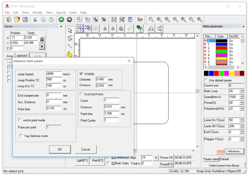
Laser parameters are in the screenshot. To cut through 1.6mm FR-4, wobble parameter is enabled (click Advanced... button)
Same parameters can be used to drill holes.
Will it solder?
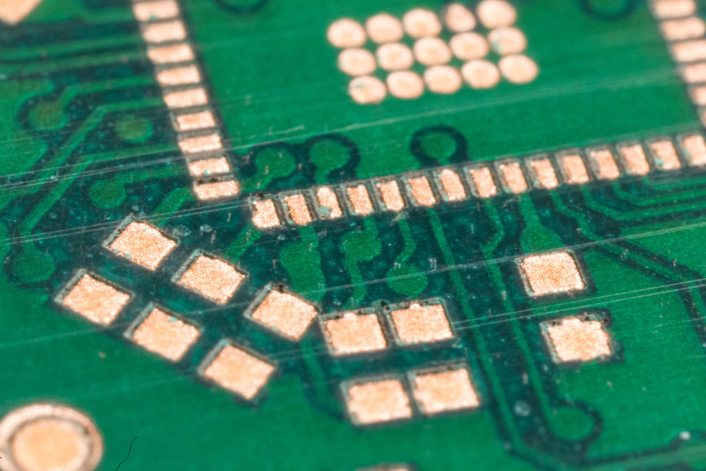
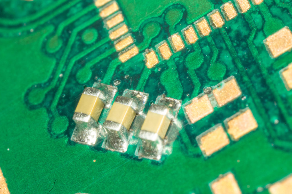
Moment of truth – 0402 capacitors soldered with hot air and after Ultrasonic cleaning look charming.
Of course bare copper will oxidize very quickly so proper care should be taken. Other than that usual soldering job.
And for your entertainment and understanding macro video with each step
Final thoughts
Well with all experiments, preparations and writing an article it took half a day. If issues with vector file import are fixed, it should be possible to have simple in 30min.
While making PCBs with 1064nm fiber laser is quick and a clean process it has some drawbacks.
- FR-4 material burns and smells, also there is a danger of having burnt resin between tracks. Good ventilation is a must!
- Isolating tracks cam be uneven. Some areas can be burnt through, some will have remaining copper.
- High energy pulsed laser would work much better, but the price of such a machine is beyond the roof.
- Stencil from stainless sheet metal can be also cut with laser. Main concern is not to overheat stainles steel. Another issue is uneven edges. This is not an issue for 0402 component pads, but smaller pads will have issues.
- During import into EZCAD, missed cleaning some geometry so some pads are incorrect. But for proof of concept and laser parameter tuning this is irrelevant.
- A good UV light source is a must. While the surface of the etched PCB can harden pretty fast, the deeper layer can remain untouched. Soldering with hot air or cleaning can open these defects spreading uncured paint.